“METHOD OF BIFACIAL CELL FABRICATION”,
“BIFACIAL PHOTOVOLTAIC CELL”,
“BIFACIAL PHOTOVOLTAIC CELL AND METHOD OF FABRICATION”
AND
“BIFACIAL PHOTOVOLTAIC CELL MANUFACTURING PROCESS”
IP Approach is pleased to present the exclusive patent for sale “Method of bifacial cell fabrication”, “Bifacial photovoltaic cell”, “Bifacial photovoltaic cell and method of fabrication”, and “Bifacial photovoltaic cell manufacturing process” which includes U.S. Granted Patent US 11,075,316 B2; US 11,387,382 B2; US 11,171,254 B2 and application patent US 20220231183 A1 and their foreign counterparts CN 108352413 B; EP 3365920 B1; ES 2939949 T3; JP 6900370 B2; WO 2017072758 A1; AU 2018399942 B2; CN 111837217 B; EP 3738139 A4; KR 102558939 B1; TWI 791081 B; WO 2019135214 A1; AU 2020284180 A1; CN 114127959 A; EP 3977523 A4; IL 288136 B2; TWI 781407 B and WO 2020240544 A1 assigned to Solaround Ltd. The IP relates to bifacial cell fabrication and, more particularly, but not exclusively, to a method of cell structure formation on a silicon substrate with fine controllable boron doping and suppressed edge shunting. The IP also relates to the field of photovoltaic (PV) cells, particularly to the field of bifacial photovoltaic cells and processes for the manufacturing thereof.
The technology disclosed provides the following advantages: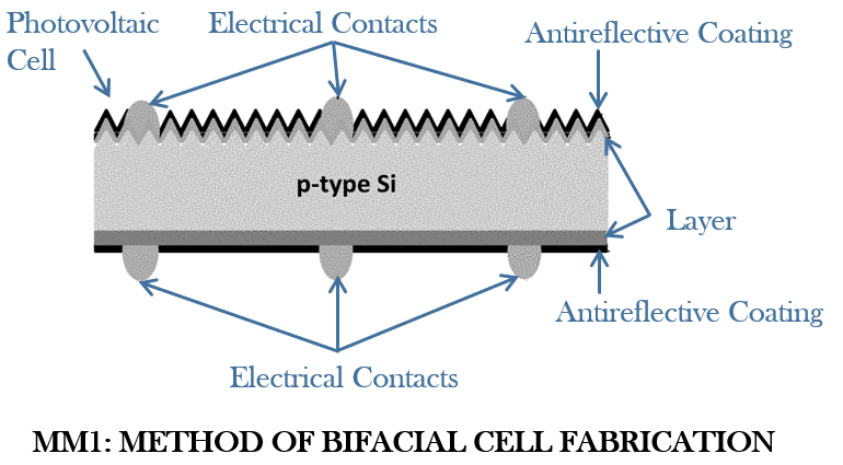
- The invention allows simultaneous or sequential diffusion of n-type and p-type dopants at controlled high temperatures (950–1050 °C), streamlining processing steps, reducing thermal cycles, and enhancing manufacturing throughput.
- The invention utilizes a thin boron-containing layer (1–35 nm) and an optional cap layer (e.g., SiO₂, SiN, SiON) to precisely control boron diffusion depth, minimize out-diffusion and cross-doping, protect against environmental degradation, and improve dopant stability during high-temperature processing.
- The invention forms optimized p⁺ layers with tailored sheet resistance (30–150 ohms per square) and surface concentration (<10²⁰ atoms/cm³), resulting in low back surface recombination velocity (<50 cm/s), reduced contact resistance under rear-side electrical contacts, and efficient back-side current collection in bifacial solar cells.
- The invention suppresses edge shunting and cross-diffusion by providing design provisions for boron-free edge zones (0.1–0.5 mm) through selective masking or post-deposition etching, ensuring reliable junction isolation and enhancing device yield without complex isolation steps.
- The invention integrates seamlessly with industrial manufacturing processes such as screen printing, sputtering, texturization, and etching, allowing high-throughput production compatible with existing photovoltaic fabrication workflows.
- The invention supports high-efficiency bifacial solar cells with front-side efficiencies exceeding 19–20.5% and back-to-front current ratios of at least 0.8, maximizing energy yield per unit area and enhancing overall module performance.
- The invention facilitates application of rear-side passivation and antireflective coatings (e.g., SiB, Al₂O₃, SiO₂, SiN, SiON), further reducing surface recombination, improving optical properties, and enabling effective light management.
- The invention maintains compatibility with cost-effective p-type silicon substrates and overcomes traditional boron doping limitations, such as lifetime degradation, through precise, low-dose, and controlled dopant profiling.
- The invention provides a robust and scalable fabrication route for bifacial photovoltaic cells with low sheet resistance in both n⁺ and p⁺ layers, excellent junction isolation, and long-term device stability, while avoiding complex or hazardous high-temperature alloying or gaseous dopant processes.
- The invention supports flexible process integration, enabling multiple sequences of applying n-type and p-type dopants, simultaneous or multistep diffusion, and compatibility with various doping techniques such as sputtering, ion implantation, PVD, and CVD.
- The invention’s cap layer functions include preventing boron out-diffusion and phosphorus cross-diffusion, confining dopants precisely, protecting layers during high-temperature and aggressive processing, enhancing chemical stability, and being easily removable for subsequent steps, thus improving doping uniformity and device reliability.
- The invention improves electrical performance by enhancing bifacial cell parameters, including increased front-side efficiency (≥19%), reduced back surface recombination velocity (<50 cm/s), lower contact resistance, minimized shunting, and formation of stable, high-efficiency junctions.
- The invention enables scalable integration of bifacial cells into modules and energy systems, supporting compatibility with diverse dopant source materials and industrial production lines, promoting broader application across photovoltaic power plants and electrical devices.
Please contact Justin Ehrlickman via email at justin@ipapproach.com or phone at 845-558-7901 to receive a Brokerage Marketing Package.

"Multifunction Test Instrument Probe"
IP Approach is pleased to present the attached exclusive patents for sale Multifunction test instrument probe which includes U.S. Granted Patent US 8,922,196 B2 assigned to Paul Nicholas Chait. The IP is designed to enhance precision and efficiency in electrical testing applications
Here are some key advantages:
- Versatile Testing Capabilities – Integrates multiple functions into a single probe, reducing the need for separate tools.
- Enhanced Precision – Features a clamp plunger and point plunger, allowing for secure connections and accurate measurements.
- User-Friendly Design – Incorporates an alligator clamp with spring-loaded jaws, ensuring ease of use in various testing environments.
- Compact & Efficient – Streamlines testing procedures, making it ideal for professionals in electrical engineering and diagnostics.
- Market Potential – Valuable for industries requiring high-precision electrical testing, including electronics manufacturing, automotive diagnostics, and telecommunications.
Please contact Justin Ehrlickman via email at justin@ipapproach.com or phone at 845-558-7901 to receive a Brokerage Marketing Package.
"System and Method for the Design of Digital Hardware"
IP Approach is pleased to present the exclusive patent for sale “System and method for the design of digital hardware” which includes U.S. granted Patents US 10,733,343 B2 and its foreign counterpart WO 2017103572 A1 assigned to Lambda Logic Ltd. The present invention relates generally to the field of electronic digital hardware design, and more particularly to the simulation and/or synthesis of such designs. The invention is particularly suited for use in the design of integrated circuits (ICs), such as application-specific integrated circuits (ASICs), and the design of programmable logic devices (PLDs), such as field-programmable gate arrays (FPGAs). The invention also relates to the field of hardware description languages (HDLs), and is suited for use by a hardware designer for the purpose of logic synthesis and/or logic simulation.
The technology disclosed provides the following advantages:
- The invention describes a tool or collection of tools for aiding the electronic digital hardware design process.
- The invention has the advantage that time-consuming simulation set ups are run once only, and are then followed by very fast subsequent simulation passes.
- The invention enables the user to use, represent and/or manipulate an RTL abstraction of the digital circuit.
- The invention constrains a design so that logical constructs can only occur within portions of code which are not conditional upon the state of any input signal. This has the advantage that each simulation pass through the design, encounters the logical constructs in the same order leading to huge simulation efficiency gains.
- The invention enables the user to simulate and/or synthesize a circuit design, and analyze the performance of a circuit constructed in accordance with the design.
- The invention enables the user to express or describe the design in an HDL specified in accordance with the rules of the invention.
- The invention allows creation of multiple simulator objects to provide advantages in situations where, for example, the user wishes to run a number of separate simulations concurrently.
- The invention avoids the simulation time overheads associated with thread or process switching.
- The invention is easier to debug because it is single threaded.
Please contact Justin Ehrlickman via email at justin@ipapproach.com or phone at 845-558-7901 to receive a Brokerage Marketing Package.
"Semiconducter Wafers with Non-Contact Inspection Capabilities"
IP Approach is pleased to present the exclusive patent for sale “Semiconductor wafers with non-contact inspection capabilities” which includes J.P. Granted Patent JP 7495764 B1 assigned to M3 Corporation. The IP relates to a wafer inspection method.
 The technology disclosed provides the following advantages:
- The invention performs a self-inspection by self-generating power such as solar power, and automatically transmits the inspection results.
- The invention provides a semiconductor wafer equipped with the non-contact inspection function.
- The invention inspects the pass/fail state of each chip in the wafer without utilizing a tester system or direct contact inspection using a probe card connected to a tester.
- The invention does not consider the limits of electrical characteristics such as S parameters inside the probe card. Hence, the frequency of the external terminals of the chips on the wafer is not restricted by the electrical characteristics of the probe card.
- The invention does not require a large measuring device such as tester connected to the probe card i.e. it eliminates the need to install them.
- The invention does not require a large-scale inspection system. Hence, it reduces carbon dioxide emissions generated during the manufacturing process of a large-scale manufacturing system.
- The invention reduces the cost required for inspection and the inspection time.
Please contact Justin Ehrlickman via email at justin@ipapproach.com or phone at 845-558-7901 to receive a Brokerage Marketing Package.
“THERMAL MANAGEMENT OF THREE-DIMENSIONAL INTEGRATED CIRCUITS”
IP Approach is pleased to present the exclusive patent for sale “Thermal management of three-dimensional integrated circuits” which includes U.S. Granted Patent US 11,710,723 B2 and its application patents US 20230395570 A1, US 20230048534 A1, 63/229,826, 62/229,842 and 18/400,219 assigned to Kambix Innovations LLC. The IP relates to integrated circuits, thermal management of integrated circuits and three-dimensional (3D) integrated circuits.
The technology disclosed provides the following advantages: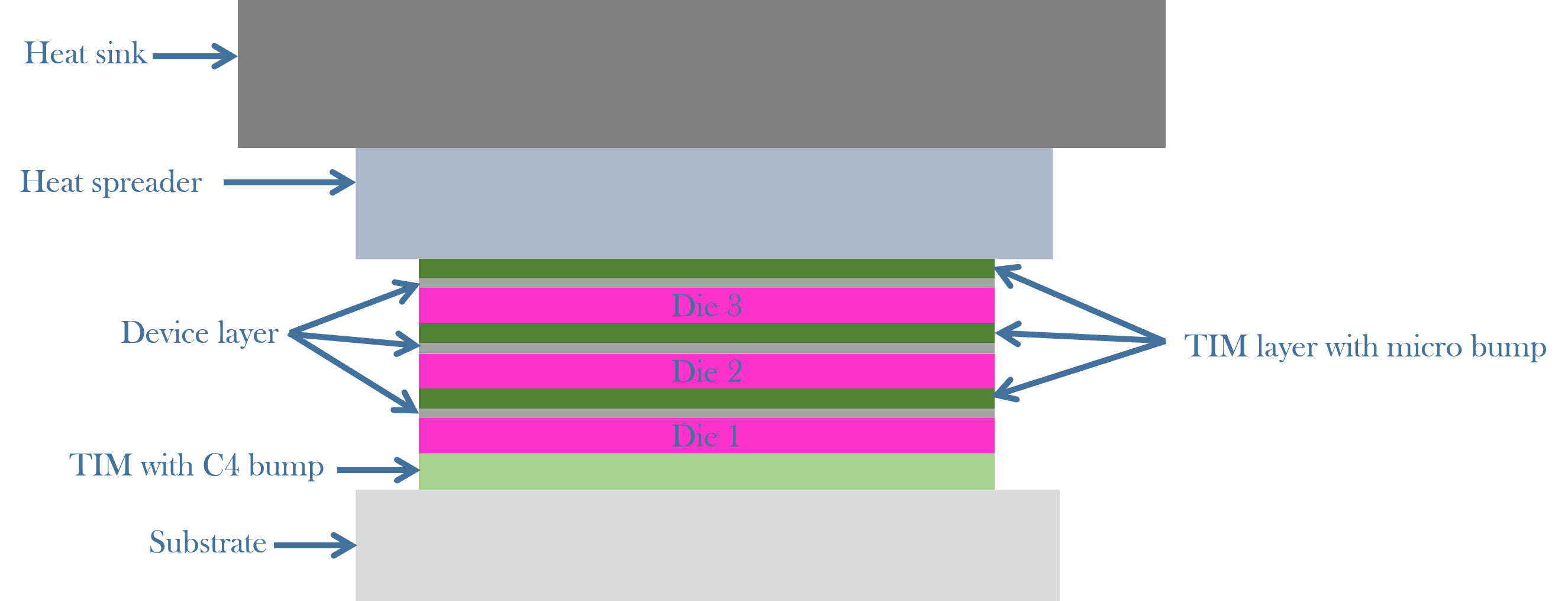
- The invention provides for the design and optimization of a composition heat spreader to improve the thermal management of a 3D integrated circuit.
- The invention provides geometrical optimization of the inserts, embedded in a heat spreader, to improve its cooling performance for 3D integrated circuits.
- The invention allows the generated heat, throughout device layers, to be transferred via conduction to a heat sink through a heat spreader.
- The invention allows the size of the heat spreader and heat sink to be larger than other layers to extend the surface area exposed to the cooling fluid and to enhance the heat transfer to the ambient fluid.
- The invention provides a high-conductivity material that can be used to boost the thermal conductance of the heat spreader to overcome the decreasing cooling capability of the heat spreader.
Please contact Justin Ehrlickman via email at justin@ipapproach.com or phone at 845-558-7901 to receive a Brokerage Marketing Package.
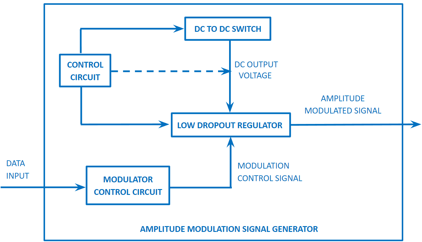
“Systems and Methods for Providing Modulation of Switchmode RF Power Amplifiers”
IP Approach is pleased to present the attached exclusive patents for sale “Systems and methods for providing modulation of switchmode RF power amplifiers” which includes U.S. Granted Patents US 9,041,479 B2, US 9,425,741 B2 and US 9,614,478 B2 assigned to Stryker Corp. The IP relates generally to signal processing and more particularly to switchmode RF power amplifiers.
The technology disclosed provides the following advantages:
- The invention is utilized in a variety of contexts like an amplifier connected to a transmitter antenna.
- The invention amplifier/antenna combination can be deployed in a medical environment. The amplifier/antenna combination can be used for activating RFID circuits located within the medical environment.
- The invention provides controlling the voltage difference between the output and the output of the low dropout regulator to maintain a minimum operating voltage difference (e.g., 0.5 volts) enables the system to maintain a high efficiency.
Please contact Justin Ehrlickman via email at justin@ipapproach.com or phone at 845-558-7901 to receive a Brokerage Marketing Package.
“Liquid Cooled Metal Core Printed Circuit Board”
IPApproach LLC is pleased to present the exclusive patents for license “Liquid cooled metal core printed circuit board” which includes U.S. Granted Patents US 9,686,887 B2 & CA 2,961,001 C assigned to Nicholas Michael D’Onofrio.
The IP relates to a system and method that cools metal core printed circuit boards by circulating a liquid coolant so that it contacts the base metal of the metal core printed circuit board.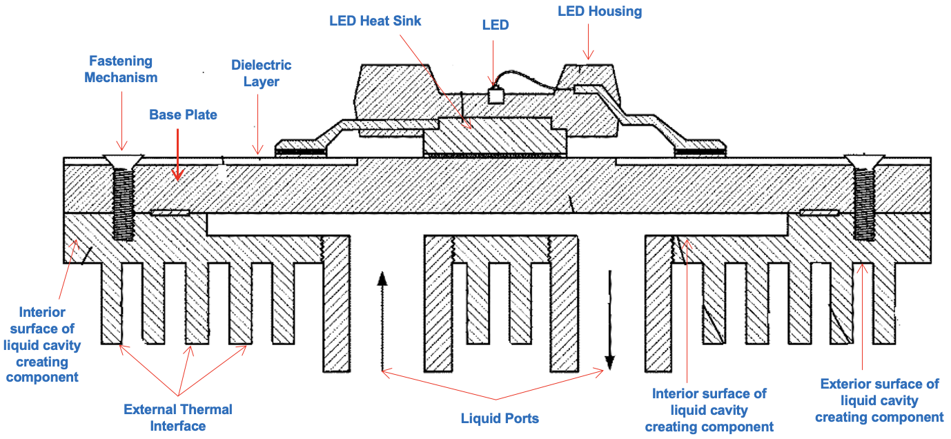
The technology disclosed provides the following advantages:
- The invention allows a liquid coolant to come into contact with the base plate of the MCPCB for cooling of the MCPCB.
- The system minimizes thermal bottlenecks between the electrical components and the cooling fluid while reducing the number of components required in previous liquid cooled electronics systems.
- The system increases thermal dissipation rates, higher possible input temperatures for cooling fluids, lower energy consumption, simplified production methods, and lower production costs.
Please contact Justin Ehrlickman via email at justin@ipapproach.com or phone at 845-558-7901 to receive a Brokerage Marketing Package.
"3-Dimensional Multi-Layered Modular Computer Architecture"
IPApproach LLC is pleased to present the exclusive patents for sale “3-Dimensional Multi-layered Modular Computer Architecture” which includes U.S. Granted Patents US 8,274,792 B2, US 9,164,555 B2, US 10,067,539 B2, and foreign counterparts EP 1,934,668 B1, CA 2,621,505 C assigned to Beyond Blades Ltd. The IP is intended for providing a computer architecture that significantly improves computer mass, volume and power densities through the use of 3-Dimensional layered structure instead of traditional 2-Dimensional Printed Circuit Board structure. The technology disclosed provides the following advantages: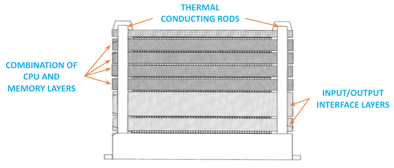
-
- The invention provides a computer architecture that significantly improves computer mass, volume & power densities.
- Provides high density computing platforms.
- The invention provides a solution for increase in device volumetric and mass efficiency, cooling problems, standardization problems and higher costs.
- The invention solves the limitation of bus speed for longer, larger latencies, cross-talk between signals, increases in noise pickup, worsen signal shape due to parasitic capacitance and parasitic inductance and electromagnetic noise that affect other devices nearby.
Please contact Justin Ehrlickman via email at justin@ipapproach.com or phone at 845-558-7901 to receive a Brokerage Marketing Package.
"Rotary SIM Tray Holder and STEM Ejectable SIM Tray Holder Assembly"
IPApproach LLC is pleased to present the exclusive patents for sale “ROTARY SIM TRAY HOLDER AND STEM EJECTABLE SIM TRAY HOLDER ASSEMBLY” which includes U.S. Patents US 10078797 B1 and US 9886654 B1 assigned to Almora LLC. The IP relates to tray holders that hold SIM or MMC cards and ejectable component assembly that allows insertion as well as ejection of SIM or MMC cards which can be used in electronic devices such as smartphone, tablet, etc.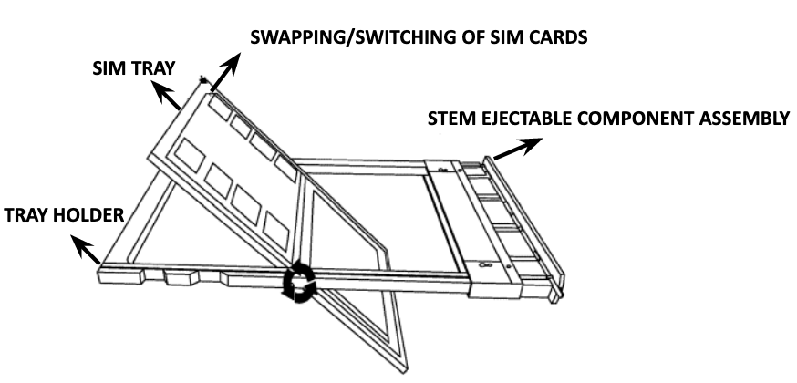
The technology disclosed provides the following advantages,
- Stem ejectable component assembly allows insertion and ejection of tray holder without using pin or needle.
- Tray holders provide convenience of putting one or more SIM or MMC cards within a device, or removing them without comprising to open the device cover.
- Tray holder is configured to hold the SIM cards in active positions or standby positions so that the SIM cards may not have to be removed or inserted in the tray holder to change.
- The handle grabber is configured to allow rotation of the tray holder to enable insertion of the rotary tray holder in an electronic device with any of two opposing faces of the tray holder oriented in a desired direction.
The target price for this portfolio is $200,000.
Please contact Justin Ehrlickman via email at justin@ipapproach.com or phone at 845-558-7901 to receive a Brokerage Marketing Package.
IPApproach has patents for sale in the following categories:
Advertising
Artificial Intelligence (AI)
Automotive & Vehicles & Trailers
Biometrics & Touch Screen
Construction
Consumer - Electrical
Consumer - Other
Data Management
Delivery & Routes
Display and Imaging
Energy
Gaming
Internet of Things (IOT)
Medical
Mobile & Telecommunications
Office Furniture / Equipment
Other
Security
Semiconductor and Packaging
Social Media
Software
Tools & Brackets
Trademark
Video
Wireless
Other - TransactionsIP